Genius Way | Plating the Future
In chip manufacturing, metal interconnects are like a crisscrossing network of ‘meridians,’ and high-end electroplating is the key process that precisely ‘weaves’ this core network.
Crafted with Precision | Driven by Innovation
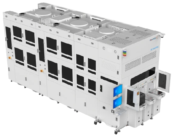
The Explora 3D is core equipment for advanced packaging, power devices, and compound semiconductor manufacturing, covering key processes such as TSV, Pillar, Bump, and RDL, helping chips achieve miniaturization and high-performance upgrades.
About Genius Way
Genius Way’s core R&D team includes several foreign experts from globally top equipment companies and overseas returnees with master’s and doctoral degrees. They deeply specialize in the semiconductor electroplating equipment business, focusing on electroplating processes for advanced packaging such as TSV, micro-bumps, and RDL, striving to become a global leader in high-end semiconductor equipments and total solutions.
Honors and Qualifications
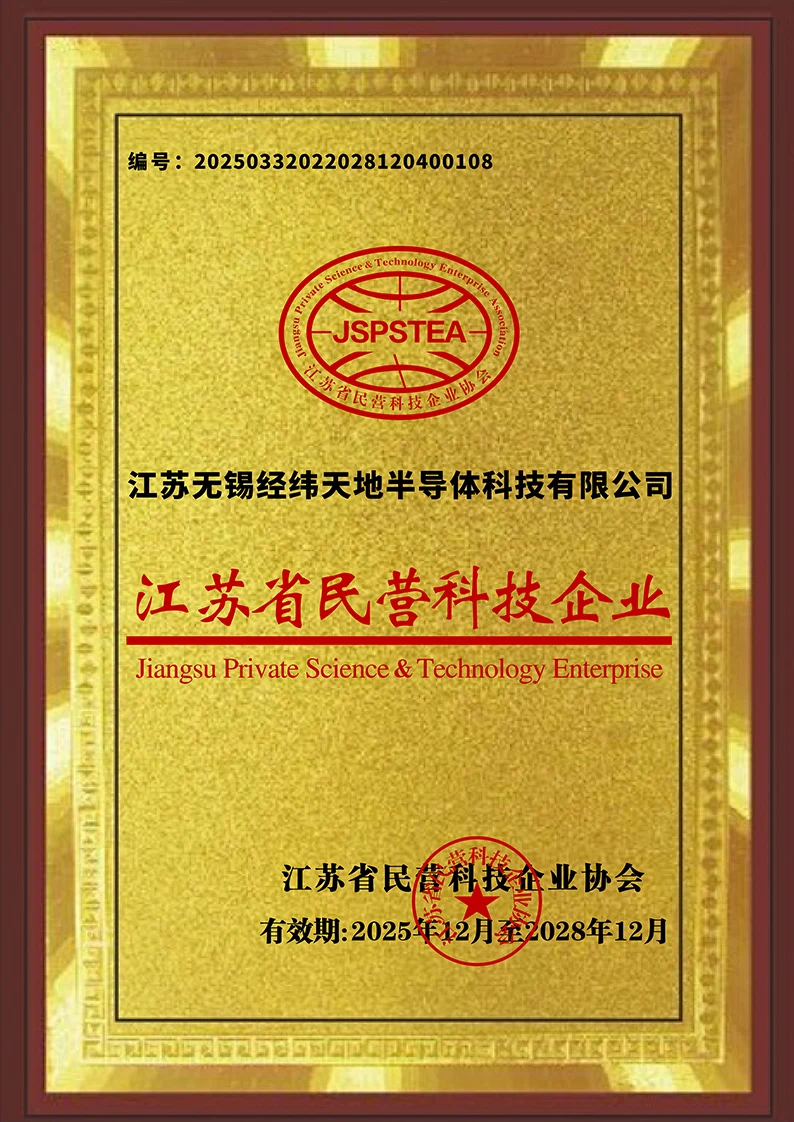
- Jiangsu Private Technology Enterprise
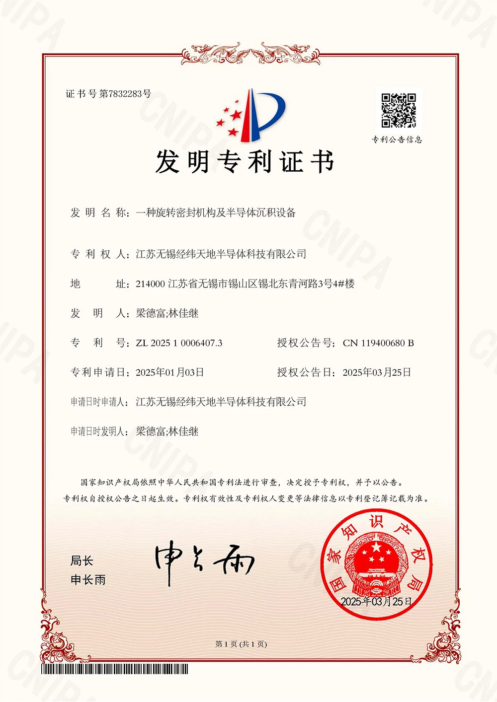
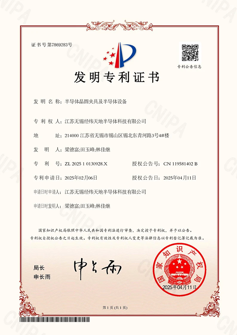
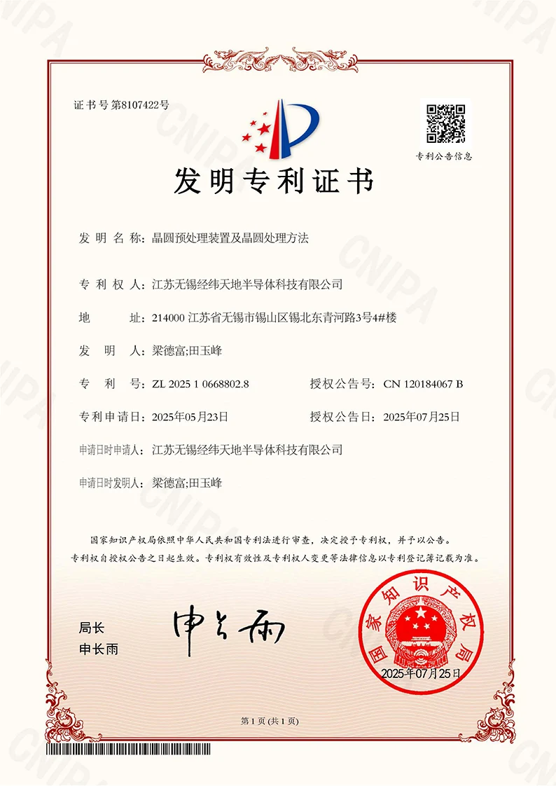
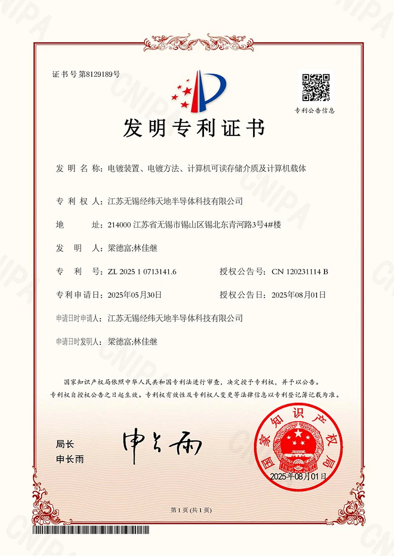
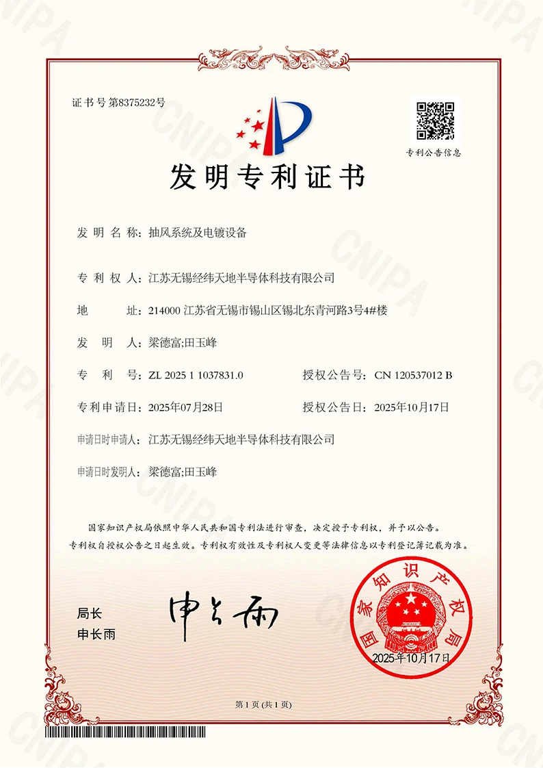
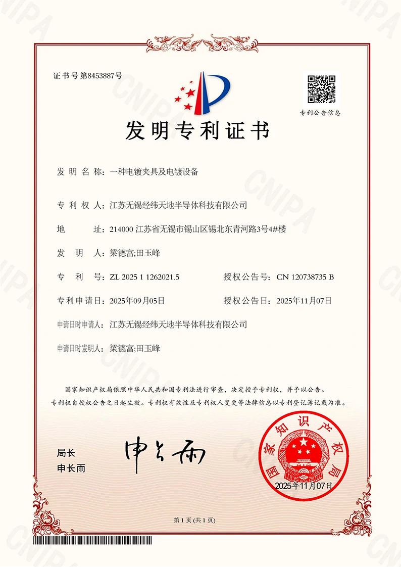
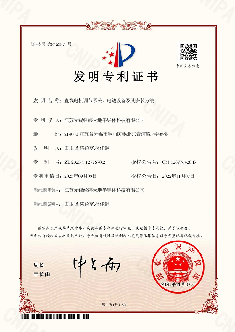
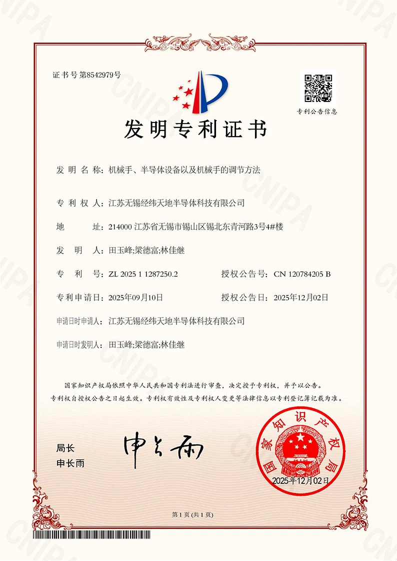
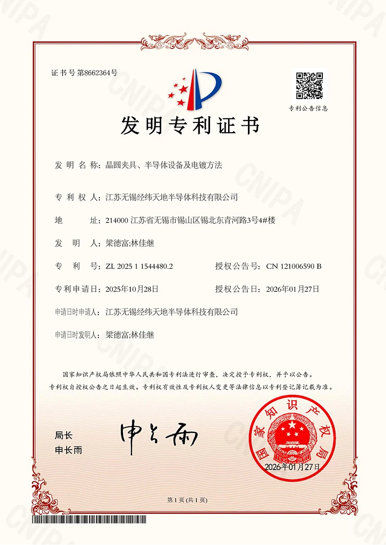
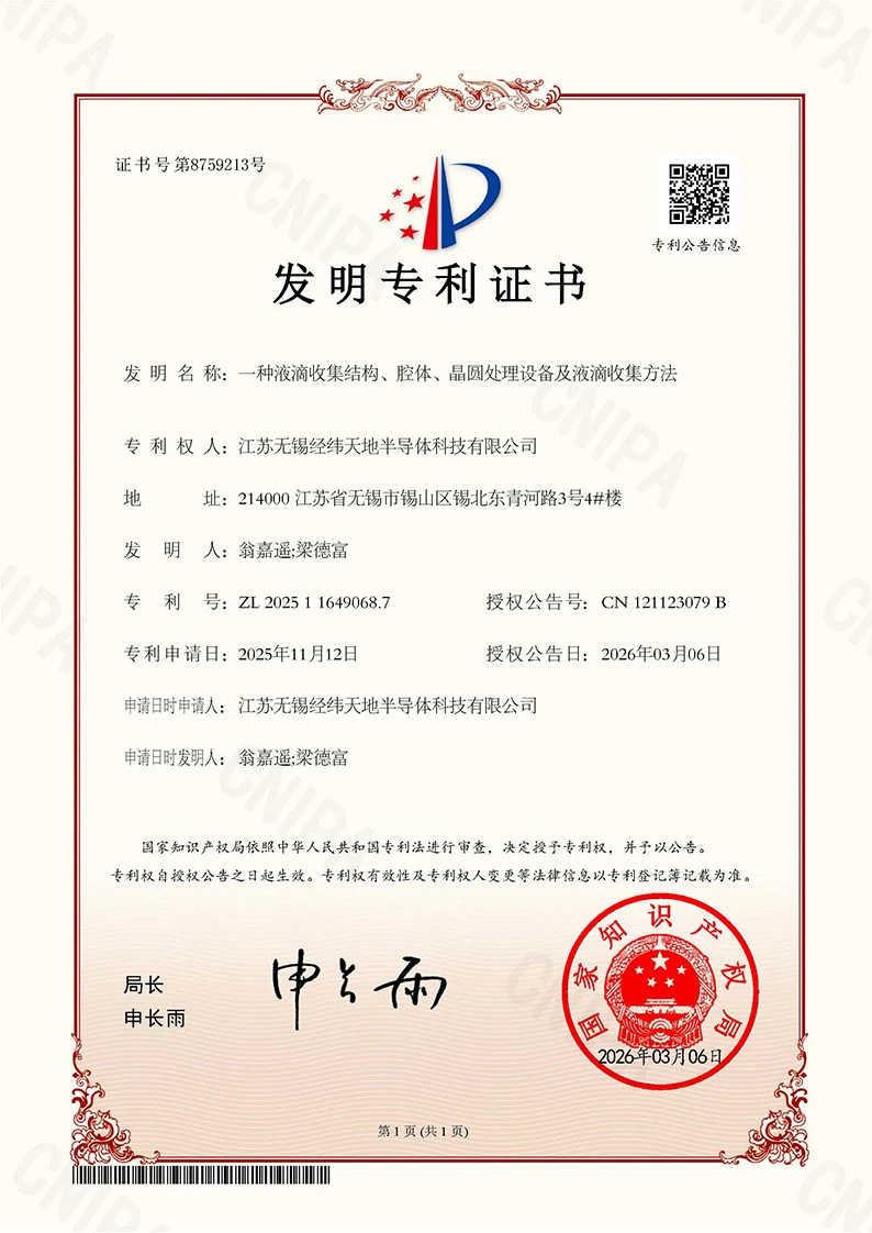
- 70 Invention Patents Application
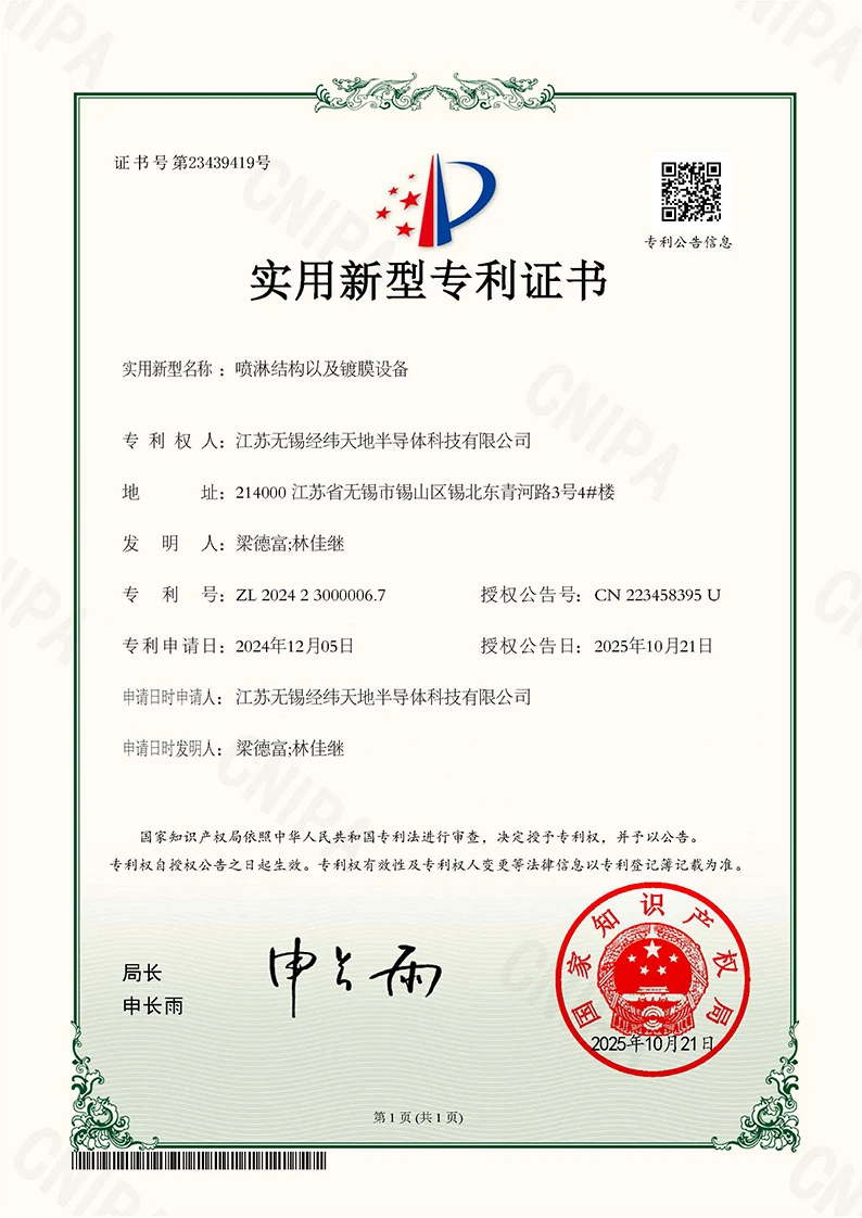
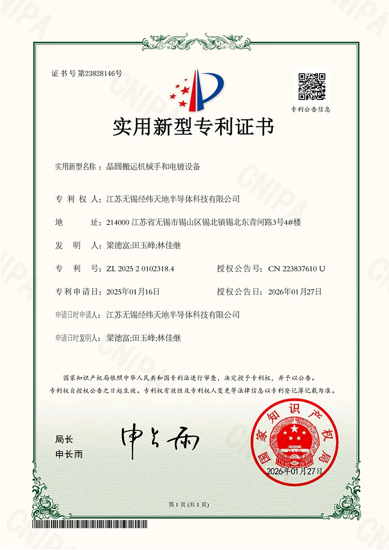
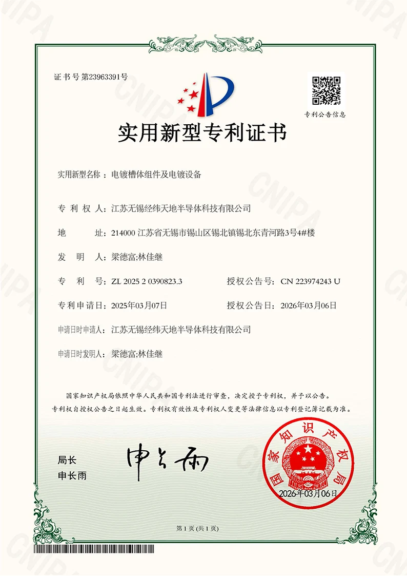
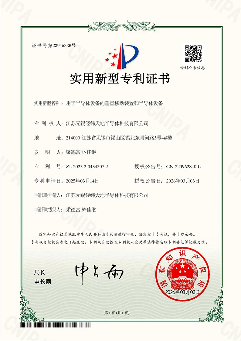
- 7 Utility Model Patents
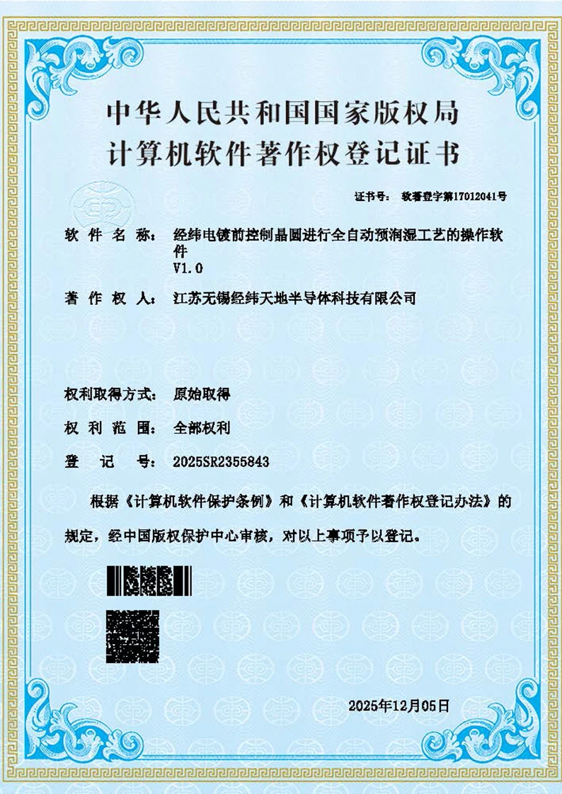
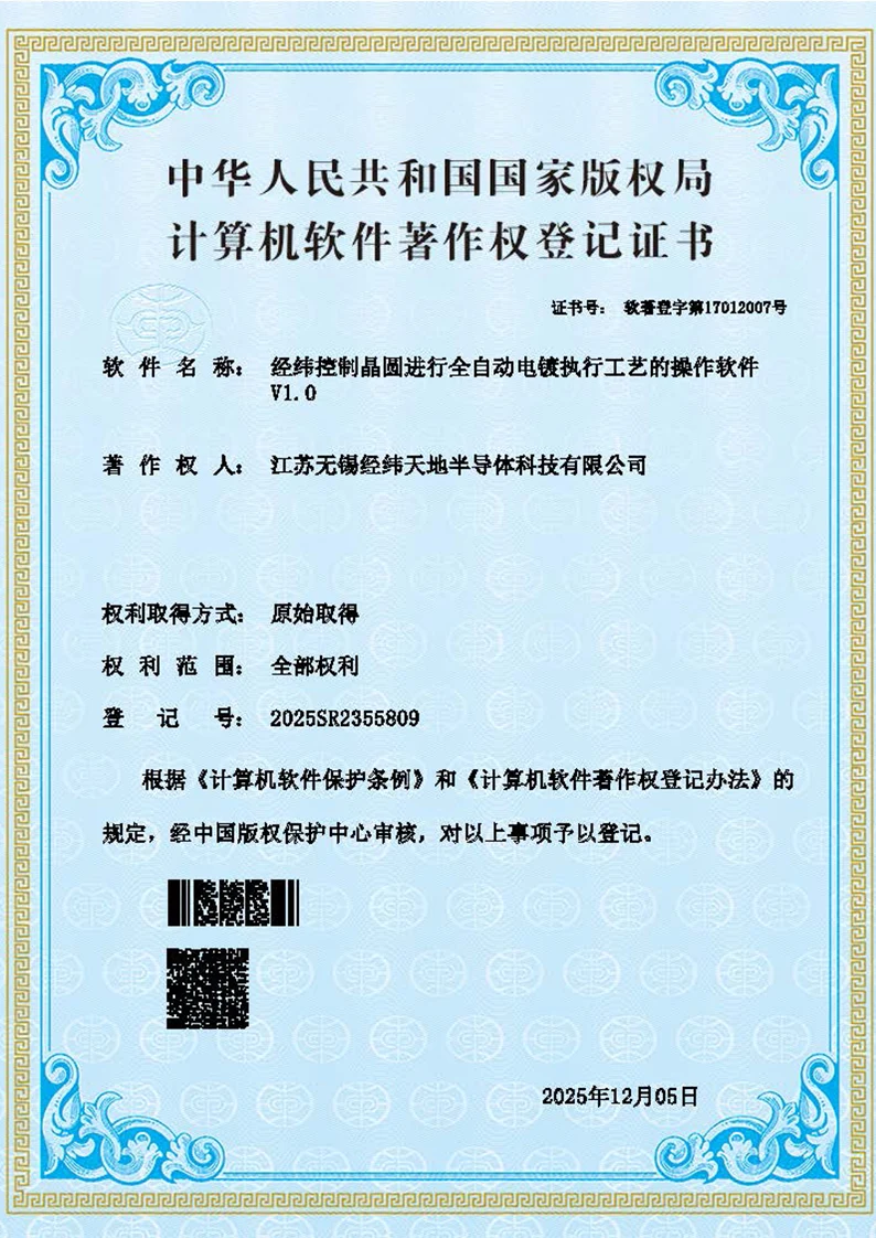
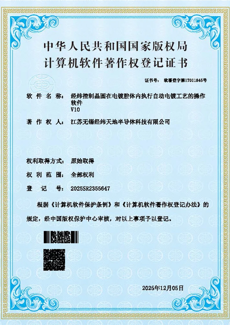
- 3 Software Copyrights
News
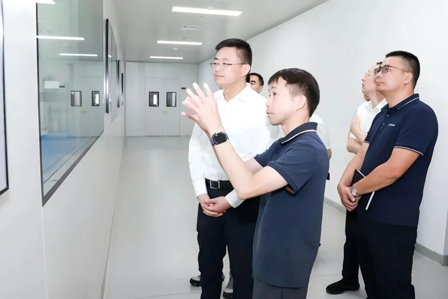
Genius Way Welcomes Xishan District Leadership for Exchange and Discussion
In June 2026, Xishan District launched a research initiative to assess the development of its semiconductor and intelligent technology industries. On the morning of June 12, Gu Wenhao, Party Secretary
Genius Way Delivers Its First 12-Inch Horizontal Electroplating System, Explora3D, to a Leading Semiconductor Customer
On May 18, Genius Way successfully delivered its first 12-inch horizontal electroplating system, Explora3D, to a leading semiconductor customer. As a key piece of equipment for advanced packaging, power devices,
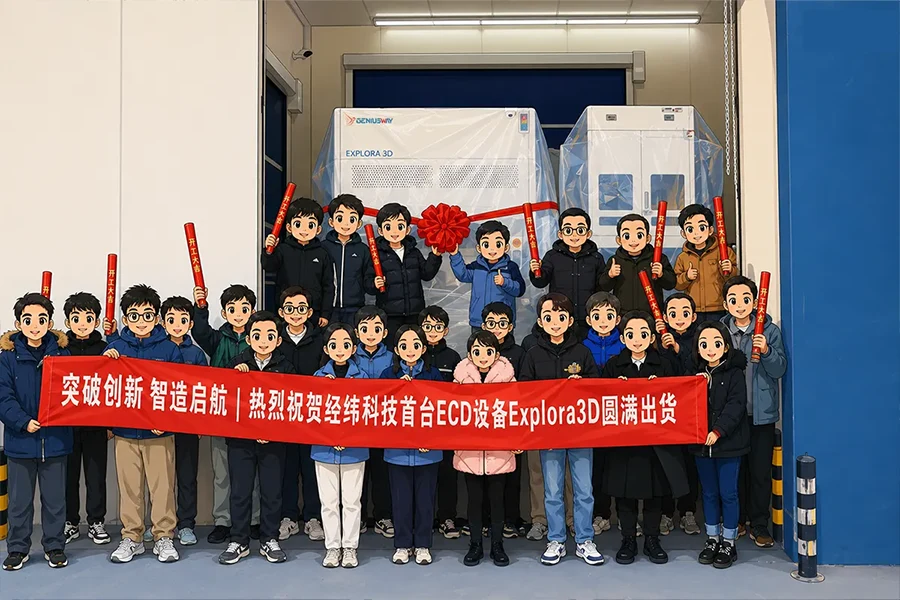
Genius Way Delivers Its First ECD System – Explora3D
On January 11, Genius Way successfully delivered its first self-developed Electrochemical Deposition (ECD) system, Explora3D, to a customer. The system integrates proprietary technologies, including a highly uniform electric field and